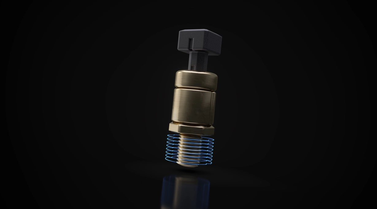
Pressure sensors
The small component with a huge responsibility
Almost two billion pressure sensors are currently produced every year. This impressive figure is due to the versatility of pressure sensors. Able to detect pressures of a few millibars all the way up to thousands, they perform vital roles in a vast range of industries. As well as the automotive and medical sectors, they can be found in consumer, industrial, avionic and other high-end applications.
How pressure sensors drive the auto sector
Standard-setting glass products for pressure sensors
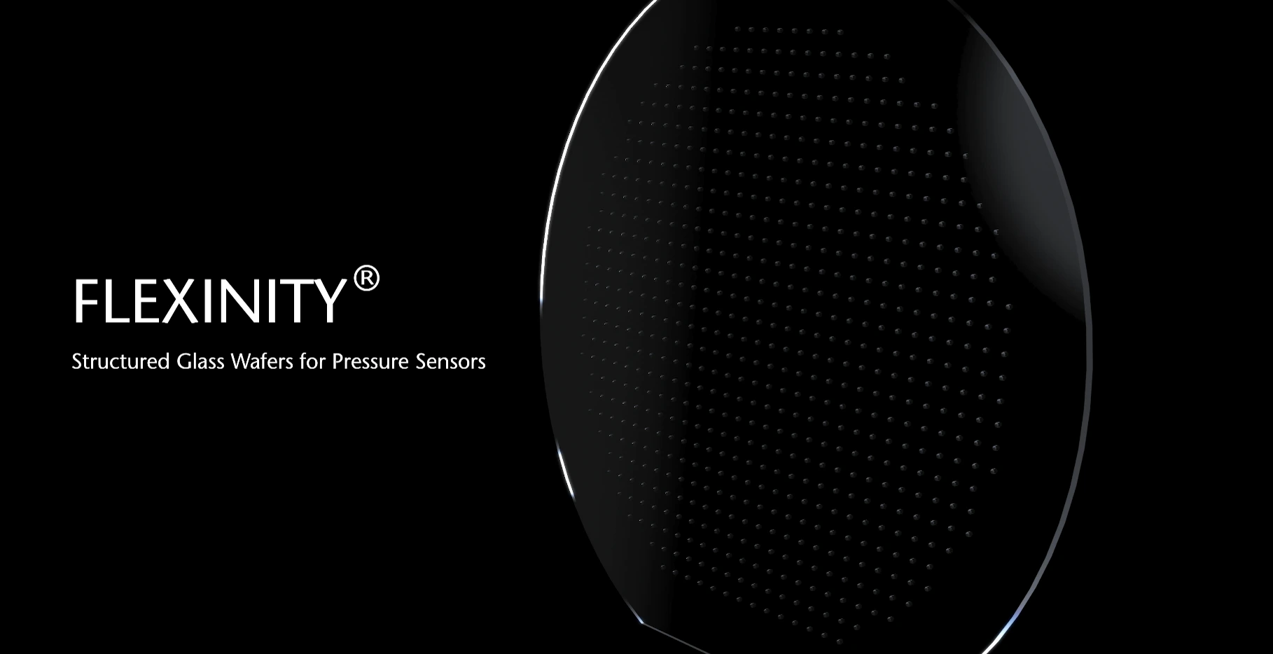
Whether processed as bare glass or structured, SCHOTT glass and glass wafers offer the ideal combination of high chemical resistance, low electrical and thermal conductivity, and outstanding structurability for highly accurate pressure sensors. The exceptionally flat and homogenous BOROFLOAT® 33 glass is perfect for the packaging of MEMS sensors thanks to its suitability for anodic bonding. If a very thin format (0.3mm or less) is required, MEMpax® can be used. SCHOTT FLEXINITY® structured glass substrates and wafers enhance functionality further with customized structures that increase effectiveness while reducing costs.
1. A huge market for a small component
Almost two billion pressure sensors are currently produced every year, a number that’s set to grow by roughly 7 % every year. The largest market for pressure sensors is in the automotive sector, which uses over half the units currently produced – around 10 for every new car. As well as performing a key role in Tire Pressure Monitoring Systems (TPMS), pressure sensors are also used to check the pressure of critical fluids such as engine and transmission oil. Add applications such as airbag activation and seat occupancy detection to check seatbelt usage, and you have one of the most important components for car safety.
2. How a pressure sensor works
Pressure sensors are a highly interactive combination of complex electronics and robust packaging materials. At the heart of a pressure sensor is the bonded MEMS silicon die, an extremely sensitive structure that includes a small and very thin membrane that bends with applied pressure. This pressure is detected by piezoresistors on top of the membrane and converted, via resistance change, into an electric signal, which is calibrated and evaluated by an application specific integrated circuit (ASIC).
Key to the overall performance of the MEMS silicon die is the pedestal below the silicon, which provides a highly accurate through-hole to guide the pressure transmitting fluid or gas towards the membrane. Glass is the ideal material for these pedestals since it has low electrical and thermal conductivity, high chemical resistance, outstanding structurability, and a coefficient of thermal expansion (CTE) that matches silicon.
3. Principle of anodic bonding
Central to the accuracy, reliability and longevity of a high performance pressure sensor is the join between the borosilicate glass packaging component and the functional silicon unit. The bond is formed electrochemically at wafer level by an anodic bonding process at a temperature of about 400 °C and voltage up to 2,000 V, uniting the chemical components in the glass and silicon. This bond needs to be strong and stable, contributing to the high electrical, thermal and chemical resistance demanded from the die packaging solution.
Advantages of glass substrates and wafers

Prof. Dr.-Ing. Roy Knechtel explains the importance of effective packaging for MEMS-based pressure sensors and why glass is the ideal material.
The key markets of MEMS* based pressure sensors are automotive, medical, industry and consumer applications. Today’s and future requirements differ from application to application within these segments. In the automotive, medical and industrial sectors, product developers focus on improving precision, long-term stability and robustness – also taking harsh environments into account.
For high-volume consumer applications, increasing demand for miniaturization at low cost is the challenge.
(*Micro Electro Mechanical System)
The packaging of the mechanical stress-sensitive silicon MEMS dies is highly important as it co-determines the overall performance of the system. For the so-called first-level-packaging there are three main tasks:
- providing stress decoupling and electronical isolation to the final module and system-level package,
- enabling a hermetically sealed reference pressure and
- providing additional protection e.g. to harsh media.
With the increasing need for improved pressure sensor system performance, glass packaging solutions are facing ongoing challenges. Smaller dies allowing higher number of dies per wafer. This require tighter tolerances in hole positioning and diameter of structured pressure sensor pedestal wafers. Best to realize in glass that is as thin as possible, to reduce the overall device thickness but keeping the stress isolation feature.
With ultra high-precision FLEXINTY® portfolio of structured glass, in combination with MEMpax®, a polish- & surface defect free ultra-thin “sister” material to the well-known BOROFLOAT® 33, a high-performance glass-based solution is now available to meet the future demands of the pressure sensor market.


